Description
Incandescent bulbs are slowing being phased out and replaced with LEDs (light emitting diode) due to their superior efficiency and size. Incandescent bulbs are easy to drive; connect a positive voltage on one terminal and a negative on the other and, viola, let there be light. LEDs are more complicated to drive as they required a very specific positive and negative voltage across (around 0.7V for a single diode) and controlled current through its terminals; called anode and cathode.
Design Files
The schematic and PCB files can be downloaded in their entirety here.
Engineering
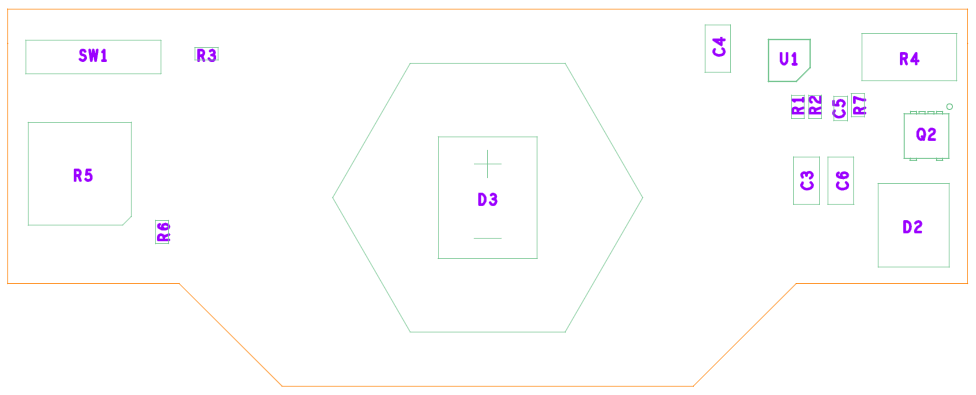
The diode used is the Luminus SST-50 15W LED mounted on a octagon shape heat sink that was purchased pre-assembled from eBay. The forward voltage of that LED is 3.2V (multiple diodes in series) but the battery voltage of my battery is 18V nominal so it needs to be reduced. The Texas Instruments LM3409 chip will “buck”, i.e. reduce, the voltage based on the RC time constant of R7 and C5. The voltage is reduced by switching the input voltage off and on repetitively then averaging that voltage with the inductor L3.
The LM3409 also limits the forward current through the LED by monitoring the current through R4. As current increases through R4 the voltage across it also increases and eventually it meets the threshold set by the voltage on the IADJ pin. The LM3409 then limits the current by reducing the time the input voltage is switched on through Q2. Q2 can be thought of as a mechanical switch but operating at a much rate much higher than you could flip your light switch on and off. In this case over two hundred thousand times per second. The resistor R5 is an adjustable resistor that allows the current through the LED to be adjusted, more current more light.
The UVLO (under voltage lock out) pin of the LM3409 monitors the voltage on the input. If the voltage on that pin falls below its internal voltage threshold of 1.24V the chip will shut off. This feature isn’t used because the required minimum operating voltage of the LM3409 is greater than the diode’s forward voltage. Additionally, the lithium battery input is 18V = 6 series 3V batteries and since lithium batteries cannot be discharged below usually 2-2.5V without damaging them the minimum input voltage would be 6*2V = 12V. This is a UVLO within the battery pack.
The switch SW1 enables or disables LM3409. The diode D2 doesn’t emit light like and LED but instead allows for current to circulate through the LED and inductor L3 during the period of time when the input voltage is switched off. Capacitors C3 and C6 help stabilize the input voltage ripple caused by it being switch off and on repetitively. Inductors resist the instantaneous change in current while capacitors resist the instantaneous change in voltage.
Since this PCB is two layer PCB and made by a service that names themselves “dirty” it’s not the highest quality circuit board. The main draw back of this cheap circuit board is its ability to dissipate heat (power loss in the components) which directly correlates to brightness of the LED. At room temperature (23°C) the current through the LED was adjusted using R5 until the circuit board was measured with a FLIR thermal camera to be 100°C. Unfortunately, the PCB does not offer enough heat sinking capability to take advantage of the full 15W power rating of the Luminus LED used yielding a less bright flashlight, yet still very bright!
Schematic
Here is the schematic whose components are referenced above. A PDF can be downloaded from here.

PCB Layout
Here is the PCB layout. A PDF can be downloaded from here.
Fabrication drawing with dimensions, stackup, drill, and revision information

Assembly top layer, shows the location of the components
Assembly bottom layer
Top copper etch layer

Bottom copper etch layer

Top pastemask layer, used to determine the location for solder

Bottom pastemask layer, there is an error here :)

Top silkscreen layer, used as visible ink indication

Bottom silkscreen layer

Top soldermask, used to expose copper

Bottom soldermask

Design Software
Cadence PCB Editor was used to design this PCB. They have a free viewer that can be used to open the .BRD file.
https://www.cadence.com/content/cadence-www/global/en_US/home/tools/allegro-downloads-start.html
Fabrication Company
One of the most hilariously named, yet entirely truthful, PCB fabrication services was used: Dirty PCBs. Even better with the nickname “Dirt Cheap Dirty Boards”. Upload the gerber artwork files pay $11.95 and get the boards in 1 month. Free shipping even!
Gerber Artwork Files
The gerber files are a industry standard digital representation of a circuit board. These files can be viewed using a free program like Gerbv if desired.
Layer Stackup
This PCB uses Dirty PCB’s standard two layer stackup. Often PCB copper layer thickness is specified in weight (oz) which is not intuitive. 1 oz of copper equals 1.4 mils thickness but does not account for additional plating all PCBs with plated drill holes (vias, pins, etc) have. 1 oz copper foil is 1.4 mils of foil + 0.3 mils of additional plating = 1.7 mils total thickness.
L1 Top - 1.7 mils
FR4 Dielectric - 58 mils
L2 Bottom - 1.7 mils
Total board thickness is approximately 62 mils with soldermask.
Pictures
Front of the PCB before assembling all of the components, the LED is the large octagon in the middle. All the drive circuit but the inductor is on the right and the on/off switch + current control is on the left

The back of the PCB only has the inductor and two connectors on the left for input from the battery

Inside the flashlight’s housing with all the components assembled. The LED isn’t a surface mount or through hole part so wires have to be manually cut and stripped to electrically connect the LED. Plastic screws and washers were used to prevent shorts from the screws eating away the soldermask.

Zoom out of the entire flashlight

Zoom out of the entire flashlight with the clear (kind of) cover

Side view of the flashlight

This picture was taken when the flashlight was on, you can see the LED array because the camera’s exposure was adjusted due to the brightness the LED target.
