Preface
This post shows three different ways to use thermal reliefs using Cadence PCB Editor. Thermal reliefs are used to ease the assembly process for printed circuit boards (PCB). Heavy weight copper layers require significant heat to reach the melting temperature of lead free solder. A quality assembly company does not require thermal reliefs; using low quality companies can result in bad solder joints.
The GIF videos below are applicable to Cadence PCB Editor 17.2 but should be similar in newer or older versions of the software.
Method 1: Globally
The global method applies thermal relief settings to the entire PCB. This is usually not an ideal method because it creates areas in the PCB that the thermal relief settings cannot be applied due to the physical shapes of the copper planes. For example, a pin connecting to a shape only on one side and using a minimum of 4 connects results in an unconnected net. See the GIF video below for an example of that.
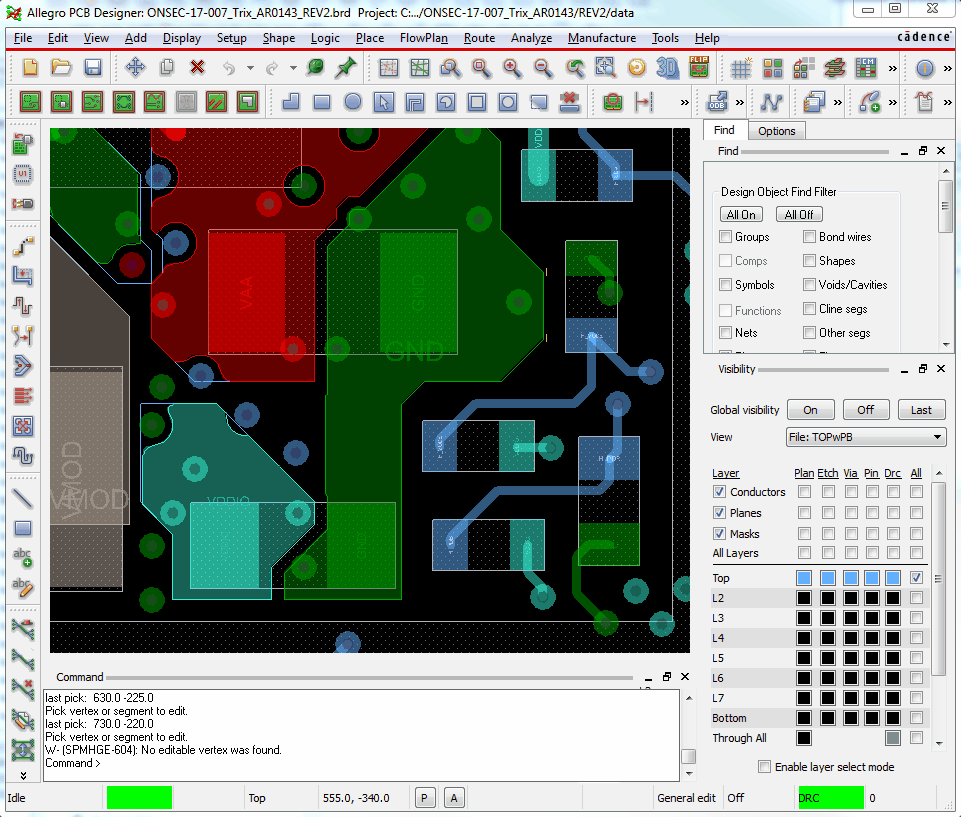
Method 2: Per Dynamic Copper Shape
The second method allows applying thermal reliefs for each individual dynamic copper shape. An example of application would be using thermal reliefs only on an internal return layer or single power shape on surface mount components as show in the GIF video below.
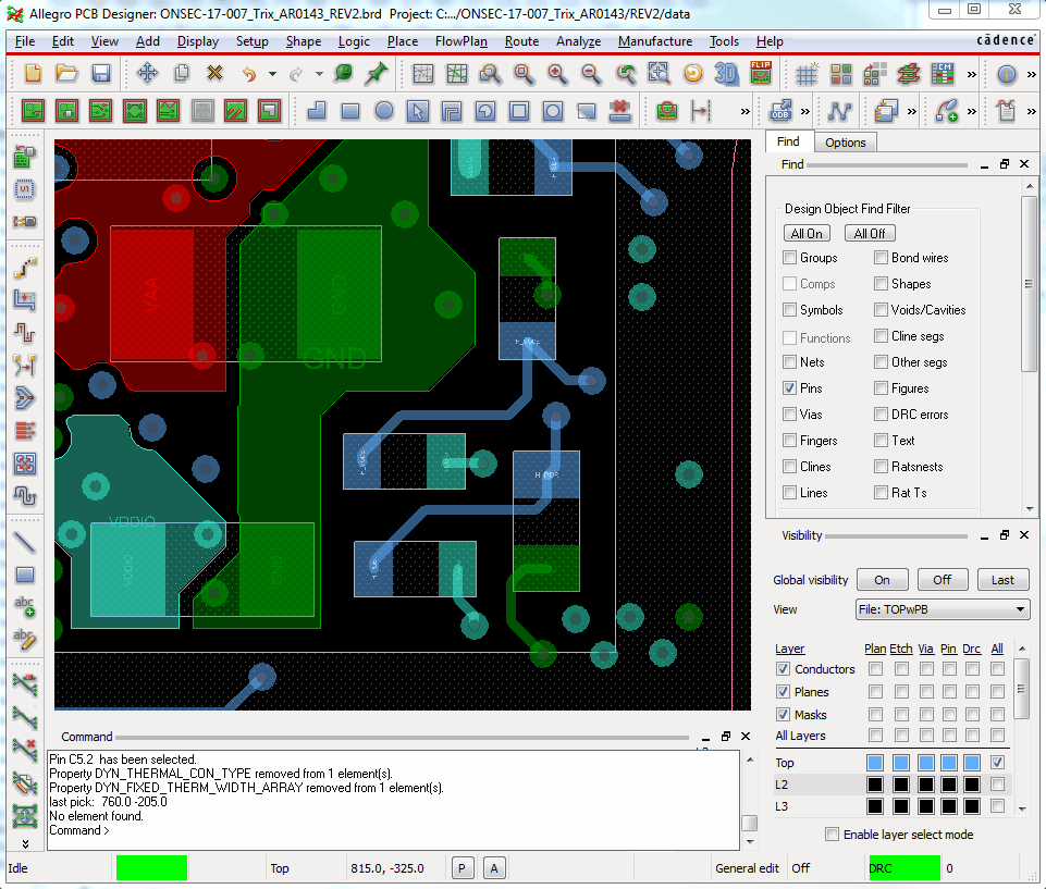
Method 3: Per Pin
The third and last method allows thermal reliefs to be added manually to individual pins. This is useful for applying thermal reliefs for a connector that requires a lot of heat to solder the mechanical pins but minimal heat for connector input/output connections. The GIF video below shows how to add thermal reliefs only on one surface mount component pin instead of the entire shape.